- 您现在的位置:买卖IC网 > Sheet目录345 > NCP1605FORWGEVB (ON Semiconductor)EVAL BOARD FOR NCP1605FORWG
NCP1217, NCP1217A
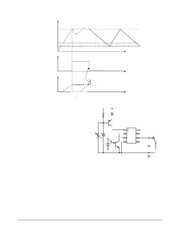
V CC
The startup current source keeps the
VCC ON = 12.8 V
VCC min = 7.6 V
device latched until reset occurs.
VCC latch = 5.6 V
Drv
Reset level
Time
Adj
Driver
Pulses
Latched--off
Time
Default
adj level
Fault brings adj above latching level
Time
Figure 24. When Vadj is Pulled Above 3.1 V, NCP1217 Permanently Latches--Off the Output Pulses
In normal operation, the Adj pin level is kept at a fixed
level, the default one or lower. As soon as some external
signal pulls this Adj pin level above 3.1 V typical, the output
pulses are permanently disabled. Care must be taken to limit
the injected current into pin 1 to less than 2.0 mA, e.g.
Vaux
through a series resistor of 5.6 k with a 10 V V CC . The
startup switch is activated every time V CC reaches 5.6 V and
maintains a V CC voltage ramping up and down between
5.6 V and 12.8 V. Reset occurs when V CC falls below 5.6 V,
e.g. when the user cycle the SMPS down. Figure 25
illustrates the operation. Adding a zener diode from Q1 base
to ground makes a cheap OVP, protecting the supply from
any lethal open--loop operation. If a thermistor (NTC) is
T
OVP
1
2
3
4
8
7
6
5
< 16 V
CV CC
Laux
added in parallel with the Zener--diode, overtemperature
protection is also ensured.
Figure 25. A Thermistor and a Zener Diode Offer
Both OVP and Overtemperature Latched--Off
Protection
Nonlatching Shutdown
In some cases, it might be desirable to shut off the part
temporarily and authorize its restart once the default has
disappeared. This option can easily be accomplished
through a single NPN bipolar transistor wired between FB
and ground. By pulling FB below the Adj Pin 1 level, the
output pulses are disabled as long as FB is pulled below
Pin 1. As soon as FB is relaxed, the IC resumes its operation.
Figure 26 depicts the application example.
http://onsemi.com
13
发布紧急采购,3分钟左右您将得到回复。
相关PDF资料
NCP1840Q8A6MNTWG
IC LED DRIVER 12CH PROGR 20QFN
NCP1910GEVB
BOARD DEMO NCP1910DEMO-B-TLS
NCP3418BMNR2G
IC MOSFET DRIVER DUAL 12V 10-DFN
NCP3418DR2
IC MOSFET DRIVER DUAL 12V 8-SOIC
NCP3420DR2G
IC MOSFET DRIVER DUAL 12V 8-SOIC
NCP3488DR2G
IC MOSFET DRVR DUAL 12V 8-SOIC
NCP5007SNT1
IC LED DRIVR WHT COMPACT 5TSOP
NCP5008DMR2
IC LED DRVR WHT BCKLT 10MICROSMD
相关代理商/技术参数
NCP1605LCDTVGEVB
功能描述:BOARD EVAL NCP1605/1396 RoHS:是 类别:编程器,开发系统 >> 评估演示板和套件 系列:* 产品培训模块:Obsolescence Mitigation Program 标准包装:1 系列:- 主要目的:电源管理,电池充电器 嵌入式:否 已用 IC / 零件:MAX8903A 主要属性:1 芯锂离子电池 次要属性:状态 LED 已供物品:板
NCP1606ADR2G
功能描述:功率因数校正 IC PWR FCTR CONTROLLER RoHS:否 制造商:Fairchild Semiconductor 开关频率:300 KHz 最大功率耗散: 最大工作温度:+ 125 C 安装风格:SMD/SMT 封装 / 箱体:SOIC-8 封装:Reel
NCP1606APG
功能描述:功率因数校正 IC LO CST PWR FCTR CONT RoHS:否 制造商:Fairchild Semiconductor 开关频率:300 KHz 最大功率耗散: 最大工作温度:+ 125 C 安装风格:SMD/SMT 封装 / 箱体:SOIC-8 封装:Reel
NCP1606BDR2G
功能描述:功率因数校正 IC PWR FCTR CONTROLLER RoHS:否 制造商:Fairchild Semiconductor 开关频率:300 KHz 最大功率耗散: 最大工作温度:+ 125 C 安装风格:SMD/SMT 封装 / 箱体:SOIC-8 封装:Reel
NCP1606BOOSTGEVB
功能描述:电源管理IC开发工具 OSPI NCP1606 100 W BOOST
RoHS:否 制造商:Maxim Integrated 产品:Evaluation Kits 类型:Battery Management 工具用于评估:MAX17710GB 输入电压: 输出电压:1.8 V
NCP1606BPG
功能描述:功率因数校正 IC LO CST PWR FCTR CONT RoHS:否 制造商:Fairchild Semiconductor 开关频率:300 KHz 最大功率耗散: 最大工作温度:+ 125 C 安装风格:SMD/SMT 封装 / 箱体:SOIC-8 封装:Reel
NCP1607BDR2G
功能描述:功率因数校正 IC CST EFCT PW FCTR CTR RoHS:否 制造商:Fairchild Semiconductor 开关频率:300 KHz 最大功率耗散: 最大工作温度:+ 125 C 安装风格:SMD/SMT 封装 / 箱体:SOIC-8 封装:Reel
NCP1607BOOSTGEVB
功能描述:BOARD EVAL NCP1607 100W BOOST RoHS:是 类别:编程器,开发系统 >> 评估演示板和套件 系列:* 标准包装:1 系列:PCI Express® (PCIe) 主要目的:接口,收发器,PCI Express 嵌入式:- 已用 IC / 零件:DS80PCI800 主要属性:- 次要属性:- 已供物品:板
